|

14 November 2011
from
NatureAsia Website
|
The controlled growth of
well-defined DNA crystals on silica substrates could
open new applications in nanoelectronics. |
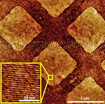
DNA crystals
grown by a silica-assisted method on patterned silica substrates
© 2011 Wiley-VCH
DNA-based nanomaterials are key
precursors for the bottom-up fabrication of a range of
high-performance nanoscale devices such as biosensors and
nanoelectronics because of their ability to self-assemble into
well-defined structures.
However, the lack of control encountered
during the deposition of these nanostructures on surfaces has
hampered their application in practical devices.
Sung Ha Park, Yonghan Roh
and colleagues from Sungkyunkwan University and the Samsung Advanced
Institute of Technology in Korea have now developed a
surface-promoted method that allows for the precise control of DNA
crystal growth on silica substrates.1
Although the self-organizing properties of DNA have been widely
exploited for constructing nanoelectronics, applications have been
restricted to single- and double-stranded DNA. However, extending
this technique to the growth of heteromaterials on substrates in
order to add functionality has proved difficult due to the lack of
control over the spatial orientation of the DNA.
To solve this problem, Park and Roh’s team used artificially
designed DNA crystals with highly periodic arrangements.
Using standard silica-based
semiconductor techniques, their approach gives complete control over
surface coverage, from 0 to 100%, and the exact location of DNA
crystal growth.
The silica-assisted growth method developed by the researchers
involves treating a silica substrate with a buffer solution
containing magnesium ions and then immersing the substrate in a
solution containing DNA. Heating the solution to 95°C and then
cooling to room temperature over 24 hours allowed the DNA to
hybridize with the substrate and form well-ordered DNA crystals.
The magnesium ions on the silica surface provide anchor points for
the DNA nanostructures, and pretreatment of the substrate lowers the
energy required for the DNA crystals to nucleate.
“This allows the formation of
crystals at DNA concentrations lower than that needed even in
free solution methods,” says Park.
By patterning the silica substrate in
advance using standard lithography techniques, the researchers were
able to produce patterns of DNA crystal (above image) that could
form the basis for nanoelectronics in applications such as organic
light-emitting diodes and solar cells.
“Our method provides a route to a
wide range of applications because the crystals could be easily
functionalized with nanowires, nanoparticles and even polymers,”
says Park.
Reference
-
Lee, J.1, Kim, S.2, Kim, J.1,
Lee, C.-W.3, Roh, Y.2 & Park, S. H.1 Coverage control of DNA
crystals grown by silica assistance. Angew. Chem. Int. Ed.
50, 9145–9149 (2011). |
article
Author affiliation
1. Sungkyunkwan Advanced Institute
of Nanotechnology and Department of Physics, Sungkyunkwan
University, Suwon 440-746, Korea
2. School of Information and Communication Engineering,
Sungkyunkwan University, Suwon 440-746, Korea
3. Samsung Advanced Institute of Technology, Yongin 446-712,
Korea
|